
A version of this post originally appeared on Tedium, a twice-weekly newsletter that hunts for the end of the long tail.
A lot of people use electronics with little to no idea of what actually happens inside of the little box they have on their desk or in their pockets.
Videos by VICE
Sure, we might talk about the chips inside of that machine, or the processing power, but rarely do we think about the connective tissue holding many of the circuits onto the silicon.
That tissue is solder, the meltable filler metal that has existed in one form or another for more than 4,000 years—long before electronics even existed as a modern context.
But in an era where that fillable metal shows up in just about everything as a way to push power through our machines and bond circuits to silicon, even if it’s not necessarily doing any of the processing of our computing, makes it important to discuss—especially as it’s considered one of the artistic elements of electronics engineering.
Let’s talk about the art of soldering. Yes, it’s an art.
Why soldering proved an important limitation for the world of technology
The technical manual Quality Hand Soldering & Circuit Board Repair sounds like the kind of work that is designed to put you to sleep—especially if you don’t know how to solder.
But if you turn it to the preface, you might be shocked to find one of the most enthralling stories this side of Chesley “Sully” Sullenberger. The 1983 crash landing of a Boeing 767 jet near Gimli, Manitoba, Canada, involved the pilot successfully “gliding” the plane to the ground because it had run out of fuel.
The crash happened for multiple strange reasons, including the fact that the country’s aviation system had recently switched to the metric system and someone forgot to tell the person who put in the fuel.
But the reason why Quality Hand Soldering author H. (Ted) Smith (yes, the “Ted” is in parenthesis) cares? The fuel error wasn’t caught right away, because the fuel gauge was on the fritz. Why was the fuel gauge on the fritz? Bad soldering, of course. It’s a dramatic example in a book about a not-very-dramatic topic.
Suffice it to say, electronics folks take their soldering seriously. Another example: Whenever soon-to-retire YouTube electronics expert Ben Heck does a soldering video, the comments are inevitably full of people criticizing both his soldering technique and the fact that, like every other American electronics engineer, he says “saw-der,” not “sol-der.” (Heck can brush off the complaints because he built this.)
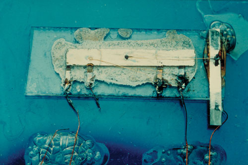
I don’t promise to teach you how to solder electronics in this piece—my interest is purely cultural, so you’ll be stuck criticizing someone else’s technique. But solder is a very important part of working on electronics, as a way of connecting and securing different kinds of electronics. But it’s always come with a bit of tension to it—because it’s not something that a newbie can pick up and perfect in a few minutes. Good soldering technique takes time.
Of course, while soldering is definitely a great way of combining one circuit with another, it’s also a quite-tedious process.
While there have been plenty of soldering innovations over the years—such as the 1896 patent received by the American Electrical Heater Company for the invention of the “electric heating apparatus,” still sold today as the American Beauty soldering iron—the process really time-consuming and can be quite annoying for someone with the wrong demeanor.
That time-consuming nature, of course, has become a long-running source of tension that’s inspired some of the most important ideas in technology history—particularly when Jack Kilby started working at Texas Instruments.
Kilby, an engineer who was stuck at work alone during the summer of 1958, decided to work on an idea he had to solve an engineering problem called the “tyranny of numbers.” Basically, the problem was that engineers wanted to make computers faster, but they were running up against theoretical limits of speed, because if they wanted to add more processing power, that meant more space-hogging circuits, and therefore more soldering. And because all that soldering was involved, it meant that every circuit was a potential human error waiting to happen.
Kilby saw a solution to the problem of too many circuits and not enough space—and it was different from the one TI was considering, which effectively involved creating modular blocks of built-in wiring. Kilby thought that if he used a semiconductor—effectively a mixture of a metal conductor and a nonmetallic insulator, like glass or silicon—he could build a component that was a circuit all on its own, no soldering required.
After doing some sketching, he tried out his idea using the metal germanium and a glass slide. He tested the tiny unit, and the crude object he built had produced a sine wave on an oscilloscope. Kilby had just invented the integrated circuit—and cut back on a good chunk of soldering required for many uses of computing.
Eventually, the microchip would vanquish the tyranny of numbers for good.

An industrial “reflow oven” for soldering. Image: Wikimedia Commons
What soldering looks like in the modern day
Of course, the creation of the microchip didn’t mean the end of soldering, either in industrial contexts, or in hobbyist ones. There was still lots of soldering involved, but not every individual circuit needed one anymore.
To give you an idea, check out this video of “8-Bit Guy” David Murray putting together a hobby computer. It’s an interesting clip if you’re into nerdy things, but the fact of the matter is, there is a ton of soldering involved in getting all those chips and transistors on the board. And, thankfully, he edits out most of the soldering.
And thankfully for the industrial revolution, we’ve figured out ways to automate soldering. Perhaps the most common such technique for speeding up the soldering process is something called “reflow soldering,” which essentially involves putting a “paste” of solder and flux—a bonding agent used to prevent oxidation—onto a circuit board, washing off the excess, then heating up the entire circuit board to a very high temperature for a very short amount of time, just long enough to melt the solder onto the circuit board.
If this sounds akin to using an oven, you’d be right—and many hobbyists (including, it should be said, Ben Heck) have been known to use ovens to reflow the solder on their machines—a technique that has also been known to bring dead machines back to life.
Certainly, if you don’t know what you’re doing, you shouldn’t even think about it. (And as solder is affected by heat, there are limits as to how effective this technique is long-term.) But this is one recipe that has made soldering just a little bit easier for the engineers of the world.
“The secret of good soldering is to use the right amount of heat. Many people who have not soldered before use too little heat, dabbing at the joint to be soldered and making little solder blobs that cause unintended short circuits.”
— A passage from a fact sheet from QST , the official magazine of the American Radio Relay League. This statement, for obvious reasons, speaks to the idea that soldering is something of an art form that takes time to get right. As a result of that, people in the engineering industry tend to care about these details—and often worry about whether younger generations will continue to learn proper soldering techniques. A 2013 blog post in EE Times that discussed the author’s experience helping an young engineer who screwed up a soldering job drew a ton of comments from people wondering what the lack of soldering skill meant for the future of the industry. “In my day—when dinosaurs roamed the Earth—all the students on my university course already knew how to solder before they’d even set foot on the campus,” EE Times’ Max Maxfield wrote.
Bon Iver: The guy who got the lead out of our electronics
If the name Iver Anderson doesn’t ring a bell, you’re missing out on knowledge about the guy who is responsible for the biggest solder-related innovation of the past 50 years—arguably, even, since the integrated circuit.
For much of the 20th century, the most common kind of solder used in a number of contexts (including in many electronics) was a mixture of tin and lead—an attractive combination for soldering uses because the two materials together had a melting point of 370 degrees Fahrenheit, a rate low enough to easily be made malleable. However, lead’s toxic nature meant that it was a problematic material to use in many cases, and in 1986, lead-based solder was one of the materials banned for use in plumbing as part of the US Safe Drinking Water Act.
Around that time, Anderson had already received his first patent involving molten metal—specifically a process of generating fine sprays of molten metal in the production of metal powder.
An engineering professor and employee at the US Energy Department’s Iowa-based Ames Laboratory, located on the campus of Iowa State University, Anderson was in just the position to help with this problem. For years, his role in the laboratory has been interested in producing fine metal powders, and played a key role in a number of innovations related to the production of such powders.
“In a word, it’s neat. I get to play with liquid metal,” Anderson said of his work in a 1997 Des Moines Register interview. “It looks tantalizingly like water that you could touch with your finger … but because it’s very dense, it flows in different ways than water.”
In 1996, he and his colleagues received perhaps the most important patents in their entire career for the invention of a lead-free solder created with the combination of tin, copper, and a small amount of silver. While the Ames Laboratory wasn’t the first to produce a lead-free replacement, the solution it came up with was stronger, and had a smaller “mushy zone”—the temperature range in which the material is a combination of solid and liquid—which made it ideal for electronics.
And while the melting point of the solder is higher than that of lead-based solder—around 423 degrees Fahrenheit—it was coming at a time when higher performance material was needed anyway.
“As microelectronic technology continues to evolve, microprocessors are becoming more complex and in all likelihood will generate more heat and increase thermal strains in electronic and circuit solder joints,” the patent stated. “Moreover, the service environment of electronic solder joints in all probability will become more severe.”
The invention had a huge amount of value based on what it did, but it was the regulatory prowess of the European Union that likely ensured the material would become a key part of many electronics around the world.
In 2003, the EU adopted a measure called the Restriction of Hazardous Substances Directive, which required that heavy metals be replaced with safer alternatives. And with many electronics entering the European market from around the world, that meant that lead-free solder would become an essential element of many digital electronics.
“I think the statistics are something like 4 billion cell phones in the world, and really, all of them are soldered with lead-free solder,” Anderson explained in a recent Ames Laboratory promotional clip.
According to IPWatchdog, 70 percent of the electronics sold globally use lead-free solder, earning Ames Laboratory and Iowa State University $58 million in the years before the patent expired in 2013.
That’s a massive amount of influence, of course, and Anderson was named to the National Inventors Hall of Fame, even as he’s continued to innovate in all forms of powdered metal.
In a recent article discussing his work on creating a titanium metal powder that is expected to prove useful in 3D printing, he summed up his career as such: “The ability to make impossible shapes out of incredible alloys is my mission in life. I want to work on ways to get this done.”
He set the stage for that work with solder.
As soldering celebrities go, you can’t do much better than Jessa Jones, who became an icon of the repair community a couple years back after taking on Apple in the public sphere.
Jones, a onetime geneticist with a skill at working on tiny objects, has become perhaps the best-known practitioner of microsoldering, the process of repairing the circuits on very tiny devices. It’s a skill that’s necessary to fix the numerous modern devices that rely on the fact that Jack Kilby’s big idea allowed manufacturers to shrink the integrated circuits to almost atomic sizes. It’s something she stumbled into after deciding to take a stab at fixing the family iPad herself—successfully, by the way.
The DIY repairers at iFixit noticed her work and collaborated with her on a series of videos about how microsoldering works. Her skill helped ensure that her business, iPad Rehab, would be known far beyond the city limits of Mendon, New York.
Jones has used her skillset to fix a whole lot of phones among other things, and in the midst of those fixes, she stumbled upon a problem with the iPhone 6 Plus, where a part of the touchscreen would stop working. Jones was able to diagnose the problem, which she called “touch IC disease,” and explain it in a detailed blog post. The work of Jones and others helped push Apple to launch a repair program to fix the issue.
Jones, thanks to her trusty tools and engineering know-how, was on the front line of an issue that forced the biggest company in the world to take notice. And if it wasn’t for her soldering know-how at scales even most engineers would struggle with, perhaps we wouldn’t have had her diagnosis.
In a lot of ways, she’s at the vanguard of modern-day soldering, a technical process that in the right hands might as well be considered an art form. No matter how tiny those “hands” actually are.
More
From VICE
-

Denise Truscello/WireImage/Getty Images -

A stack of modular Mesh Home Batteries – Credit: Pila Energy -

Gemini on a smartphone – Photo Illustration by Thomas Fuller/SOPA Images/LightRocket via Getty Images -

(Photo by Shirlaine Forrest / WireImage via Getty Images)